Under construction....
The general purpose input/output board (GPIO) board comes partly assembled. All the surface mount devices have already been soldered to the board. These include the processor, and the serial and CAN communication circuits.
There are a number of steps remaining to build your general purpose input/output board. These go under the main stages of:
Under construction...
Assemble and Test the Base Circuits
When you purchase a GPIO kit, the components typically arrive individually packed, with part numbers. As a result, while you should verify that you have received all you ordered, it is not necessary to identify each item by color, markings, etc.
If you have questions about the specification or appearance of any item, check the part number (listed in {} brackets here) at the Digi-Key site (www.digikey.com) first. Entering the part number in their search engine will give you access to both the catalog information and the data sheet from the manufacturer.
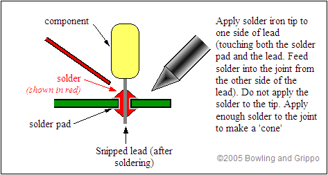
To assemble any of these electronic kits, you will need a soldering iron, some solder, and a few other useful accessories. A 15 watt pencil iron will work fine, however a 25 watt iron heats up faster. Get some small solder. For example, you can use 0.75mm resin solder (~0.030") which really helps to put just the right amount of solder in just the right places. You do not need to use silver solder for MegaSquirt. Make sure to let the soldering iron get hot before using it. A hotter tip makes for quicker cleaner joints, and less heat in the components, because the temperature of the lead reaches the melting point of the solder before the component has had much time to heat up (though letting the iron heat for a while also tends to shorten the useful life of the tip). Let it sit 'powered-up' for 10-15 minutes before trying to use it. The solder should melt nearly instantly if touched to the tip.
Never try to paste solder on a joint using excess solder on the tip. Keep the tip clean, and heat the joint (try to get the tip right at the joint between the lead and the PCB) and hold the solder against the other side of the joint until it starts to melt. Feed in just enough solder to get a bit of a "cone" around the joint, and you are done.
Get a braided copper solder wick as well - you will be glad you did! It is very useful for removing components and cleaning up excess solder. Before plugging in your soldering iron, be sure you read and understand the assembly instructions that follow.
Note: The semiconductor components in GPIO board are sensitive to electrostatic discharge {ESD). To reduce the potential for damage from ESD, some care is needed. Interestingly, you cannot even feel an ESD shock unless the voltage exceeds 3000 volts, far more than enough to destroy some of the GPIO board's components. ESD events do not always destroy an electronic component immediately on the first occurrence, making any eventual failure of your GPIO board very difficult to troubleshoot. Where possible, make use of anti-static controls and material handling techniques, i.e., wrist-band grounding straps, anti-static foam and anti-static bags, grounded workbenches, anti-static mats, etc. Avoid handling semiconductor components more than necessary. If you are not wearing a wrist-band grounding strap, discharge yourself by touching grounded metal before handling ICs and equipment. This is especially important in the winter after taking off or putting on any garments, for example, sweaters and coats. The material of your clothing also has an effect, as materials like silk and some artificial fibers produce a lot of "static electricity". Most commercial carpets contain a high percentage of artificial fibers, which are prone to producing static. Where possible, try to keep the room humidity at 50% or higher to reduce static problems, or use a product such as "Static Guard".
Your GPIO board uses a number of components. These components are installed on the silkscreen side of the PCB, and in most case it will be easiest to solder them from the other side of the board. Electrically, the soldering works fine from either side, but as you get more components on the board, it gets harder to solder on the components side, forcing you to use the other side for soldering. There are three ways you can be sure of putting the right components in the right places with the right orientation. Most electronic parts have a standardized scheme for identification.
There are a large number of cryptic designations in building a GPIO board. Many of these have the form of a capital letter followed by a one or two digit number. These indicate components that are installed on the GPIO main board (or stim, etc.) and are specific to each PCB. So R9 means resistor (R) number 9. Note that the main board may have an R9, and the stim might too, but they are different. Here are some examples:
A. Base Circuits:
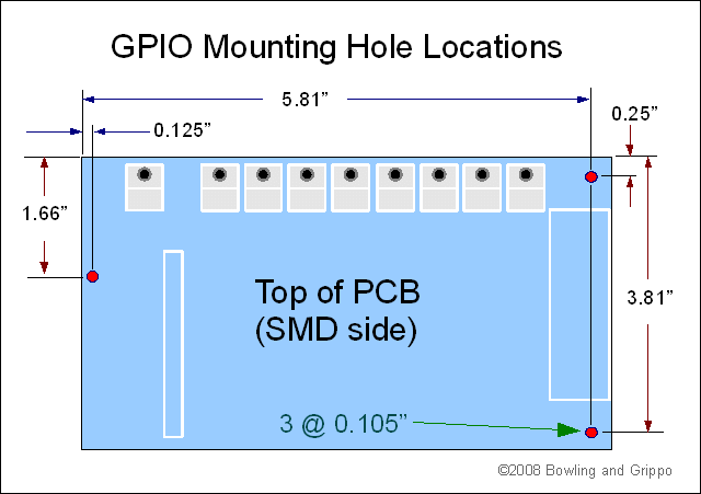
Note that if you wish to mount the GPIO PCB in a non-standard case, three mounting holes are provided:
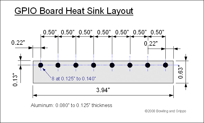
Because aluminum isn't typically sold in 5/8" widths, you may have to cut down wider aluminum (¾" or 1") to get a heat sink that will to fit.
The easiest way to get the hole spacing right is to transfer the holes from the PCB to the aluminum strip by placing them together and using a felt pen to mark the hole locations on the aluminum strip through the PCB.
Be sure to allow enough room for the aluminum strip to fit in the case, and allow enough room so that it won't contact the component leads. Make sure the heat sink rests up against the case when installed to get the thermal contact between the case and the heat sink. Sand both sides of the heat sink to ensure there are no burrs.
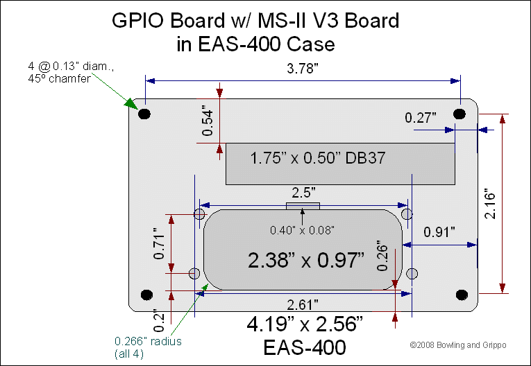
The end plate material should be 0.080" to 0.125" thick. The Ampseal connector is sealed internally in this configuration, but the enclosure itself is not sealed (because of the DB37 as well as the tolerances of the end plate to the outside flange of the Ampseal connector (rather than screwed to the face of the flange).
The GPIO board fits in the bottom slot of the its half of the case, while the V3 main board sits in the second from the bottom slot of its part of the case. Note that the DB37 and Ampseal connector are very close - there isn't much material left (~0.070"), and you will have to be careful to avoid damaging this area while machining. Thicker material will make this easier, of course.
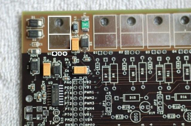
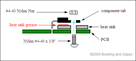
It has its own location among the SMD components in that corner of the board. You have to bend the leads to a 90° angle so the regulator can site flat against the board, then solder it and screw it the board with a #4-40 nylon bolt and nut (with heat transfer compound (aka. 'heat sink grease') between the regulator and board). You do not need a separate heat sink for the voltage regulator (shown in the diagram below), the voltage regulator can be mounted directly to the PCB (with heat sink compound), as long as you are not using the 5Vref supply for powering off-board accessory circuits.
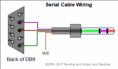
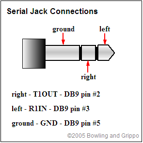
Assemble a serial connector cable:
You have a choice here. You can bring the serial communications out a serial jack (with a 2.5mm mini stereo jack, which is convenient) or you can bring the serial communications out the Ampseal connector (which offers the possibility of weather sealing).
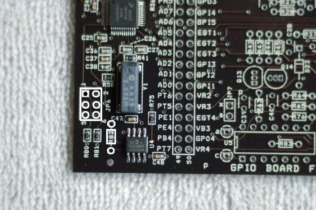
Depending on what you want from your GPIO controller, though, you may end up using the boot header to eventually to load code. To load new code, you put jumper on the two pins on JP5 with no power applied to the board, and once the jumper is in place apply power to the board and use the downloader program.
Some people have put a momentary switch (normally open - NO) across the boot header, and place the switch so they can go into bootloader mode simply by pressing this switch while powering up, without opening the case. (If you do this, be sure it can't be pressed accidentally.)
The circuits and processor pins all connect through the 25x2 header on the GPIO board, which is labeled with the circuit (on the right) and the processor port/pin (on the left). For example, an adjacent pair might be PA0/VB2 meaning that if you jumper those pins, CPU port AD pin 0 will be connected to circuit VB2, which in turn is connected to Ampseal pin 12.
The CPU has six I/O ports with a total of 25 free pins (those not used for serial, CAN, or bootloader functions). The ports are:
However, the point of having the 25x2 header is that you can move the circuit to any pin with a jumper, if you need to do this to suit your application.
Once you have decided which circuit will be dedicated to each processor pin, solder each of the header pins/jumpers as appropriate from the bottom side of the board (you can use tape to hold the header in place while it is upside down). For now, do not install the 'slide-on jumpers' on all the applicable circuits (see the table near the top of this document). You can do that after checking the circuits at the end of the build process.
You can use snipped off leads as jumpers instead and save several dollars on the WM8135 header and jumpers - if you are doing this, wait until the end of the build to install the remaining jumpers - and save the snipped off leads from other components as you go.
(You could install the complete 25x2 header then jumper the relevant pins by soldering wires directly to the header pins, if you prefer. Be sure not to bridge neighboring pins, of course.)
Double check that you have jumpered the correct locations.
B. Write/load the code to activate I/O circuits
Now that you have assembled the base circuits on your GPIO, you need to load the code you wish to use (MShift™ or something based on the template code usually) For example, loadable MShift™ transmission controller code files and instructions are listed here: Code Versions).To program your controller, you need embedded code, which will be found as an .S19 file. The GPIO board can load any MegaSquirt-II™, MicroSquirt™, or MShift™ code directly. Loading such code (even temporarily just to check the communications before assembling the I/O circuits) will give a 'known good' reference for testing the communications and TunerStudio setup.
Successfully loading code will verify that CPU and serial communications circuits are functioning properly.
To write custom code for your GPIO board, you can start with Freescale's 'special edition' of its Codewarrior compiler software and the template code project. You can read more about those here:
C. Input/Output Circuits:
Most users have been assembling their I/O circuits based on the GPIO docs (linked below). There really is no 'standard build' for custom code based on the template code, as users will do different things with different circuits.The best bet for designing and setting up circuits is to follow the links from here: GPIO main page, especially these:
- General Purpose Inputs
- Resistance Sensing Circuit
- Software De-Bounced Digital Input Circuit
- Voltage Sensing Circuit
- Resistance Sensing Circuit
- VR Inputs
- EGT Inputs
- Exhaust Gas Temperature Measurement
- Using Thermocouples
- Using the EGT Circuit as a General Purpose Input
- General Purpose Outputs
- Simple Ground Circuit
- Flyback Ground Circuit
- Pull-Up Circuit
- Choosing a Transistor for an Output Circuit
- Choosing a Light Emitting Diode for an Output Circuit
- Choosing a Flyback Diode for an Output Circuit
- Choosing a Pull-Up Resistor for an Output Circuit
- Pulse Width Modulation Outputs
- High Current Outputs
You can also use the MShift™ build guide as an example for many of the circuits in building your own circuits.
To test your I/O circuits, you will find the schematics helpful (linked above, with more detailed GPIO board schematics at: www.msgpio.com/manuals/gpiohw.htm). You need to be sure that the processor pins never see more than 5.6 Volts absolute maximum. This is the second reason for the 25x2 header - you can put off installing the jumpers until you have completed the circuits and have external connections for them. At that point you can verify that the circuit side of the pairs of header pins does not have excessive voltage on it. This will safeguard against accidental processor 'melt-downs'. Once you are sure everything is right (you do get a signal, and the voltages are in a safe range) you can install the jumper(s).