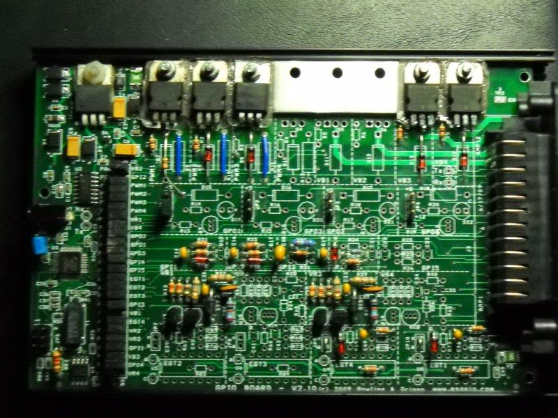
MegaShift™ GPIO v2.10 4L80E Build Instructions
These are the draft build instructions for the v2.10 GPIO board from Bowling and Grippo when using it with the MegaShift™ transmission controller software for the GM 4L80E transmission (other transmissions may be similar but may require some changes to suit their requirements).
This page specific to the 4L80E transmission was created from the 4L60E page by Dave Hjort, our many thanks for that! Dave provided the 4L80E specific instructions and photos. The parts required are detailed here: 4L80E bill of materials. Click these links to go to the:
In these instructions, we will build one type of circuit at a time. We start with the base circuits (power, CAN and serial communications circuits), then move onto the input/output circuits: GPOx, VBx, PWMx,
GPIx, EGTx, and finally the VRx circuits.
|
MShift
Function | Processor
Port | GPIO
Circuit | GPIO AMP
Connector Pin |
| Output1 (Sol A) | PE4 | VB3 | 23 |
| Output2 (Sol B) | PM2 | VB4 | 35 |
| Output3 (Sol32) | PT1 | PWM4 | 34 |
| PC | PT2 | PWM3 | 33 |
| TCC | PT3 | PWM2 | 32 |
| LED1 | PM4 | GPO1 | 10 |
| LED2 | PM3 | GPO2 | 7 |
| LED3 | PM5 | GPO3 | 8 |
| LED4 | PB4 | GPO4 | 9 |
| Input 1 (switchA) | AD0 | EGT4 (build as GPI)1 | 26 |
| Input 2 (switchB) | AD1 | GPI2 (jumper at 25x2 header) | 6 |
| Input 3 (switchC) | AD3 | EGT3 | 25 |
| Paddle UP | PT6 | VR2 | 15 |
| Paddle DOWN | AD6 | GPI5 | 4 |
| VSS | PT0 | VR1 | 2 |
| Temp Sensor | AD2 | GPI3 | 30 |
| Brake Sense | AD7 | GPI4 | 3 |
| Speedo Output | PT4 | PWM1 | 31 |
| Spare Output1 (SP1) | PT7 | VB1
(jumper at 25x2 header) | 11 |
| Spare Output2 (SP2)/Output4 | PA0 | VB2 | 12 |
| non-CAN MAP/TPS/MAF | AD5 | EGT1 | 24 |
| Line Pressure Sensor | AD4 | EGT2 | 27 |
| 2WD/4WD Sense/Input4 | PE1 | GPI1 | 5 |
| non-CAN tach | PT5 | VR3 | 14 |
When you purchase a MegaShift/GPIO kit, the components typically arrive individually packed, with part numbers. As a result, while you should verify that you have received all you ordered, it is not necessary to identify each
item by color, markings, etc.
If you have questions about the specification or appearance of any item check the part number (listed in {} brackets here) at the Digi-Key site (www.digikey.com) first. Entering the part number in their search engine will give you access to both the catalog information and the data sheet from the manufacturer.
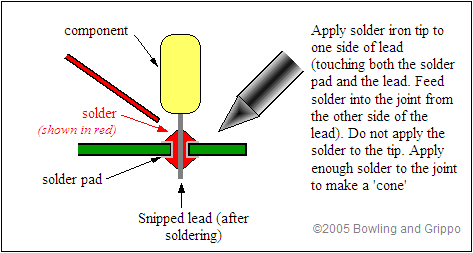
To assemble any of these electronic kits, you will need a soldering iron, some solder, and a few other useful accessories. A 15 watt pencil iron will work fine, however a 25 watt iron heats up faster. Get some small solder. For example, you can use 0.75mm resin solder (~0.030") which really helps to put just the right amount of solder in just the right places. You do not need to use silver solder for MegaSquirt. Make sure to let the soldering iron get hot before using it. A hotter tip makes for quicker cleaner joints, and less heat in the components, because the temperature of the lead reaches the melting point of the solder before the component has had much time to heat up (though letting the iron heat for a while also tends to shorten the useful life of the tip). Let it sit 'powered-up' for 10-15 minutes before trying to use it. The solder should melt nearly instantly if touched to the tip.
Never try to paste solder on a joint using excess solder on the tip. Keep the tip clean, and heat the joint (try to get the tip right at the joint between the lead and the PCB) and hold the solder against the other side of the joint until it starts to melt. Feed in just enough solder to get a bit of a "cone" around the joint, and you are done.
Get a braided copper solder wick as well - you will be glad you did! It is very useful for removing components and cleaning up excess solder. Before plugging in your soldering iron, be sure you read and understand the assembly
instructions that follow.
(Note that there is also an excellent tutorial for the assembly of general electronic kits here: www.mtechnologies.com/building/atoz.htm.)
Note: The semiconductor components in MegaShift/GPIO are sensitive to electrostatic discharge {ESD). To reduce the potential for damage from ESD, some care is needed. Interestingly, you cannot even feel an ESD shock unless the voltage exceeds
3,000 volts, far more than enough to destroy some of the MegaShift/GPIO components. ESD events do not always destroy an electronic component immediately on the first occurrence, making the eventual failure of your MegaShift™ GPIO very difficult to troubleshoot. Where possible, make use of anti-static controls
and material handling techniques, i.e., wrist-band grounding straps, anti-static foam and anti-static bags, grounded workbenches, anti-static mats, et. Avoid handling semiconductor components more than necessary. If you are not wearing a wrist-band grounding strap, discharge yourself by touching grounded metal before handling ICs and equipment. This is especially important in the winter after taking off or putting on any garments, for example, sweaters and coats. The material of your clothing also has an effect, as materials like silk and some
artificial fibers produce a lot of "static electricity". Most commercial carpets contain a high percentage of artificial fibers, which are prone to producing static. Where possible, try to keep the room humidity at 50% or higher to reduce static problems, or use a product such as "Static Guard".
MegaShift/GPIO uses a number of components. These components are installed on the silkscreen side of the PCB, and in most case it will be easiest to solder them from the other side of the board. Electrically, the soldering works fine from either side, but as you get more components on the board, it gets harder to solder on the components side, forcing you to use the other side for soldering. There are three ways you can be sure of putting the right components in the right places with the right orientation. Most electronic parts have a standardized scheme for identification.
There are a large number of cryptic designations in building a MegaShift™ GPIO board. Many of these have the form of a capital letter followed by a one or two digit number. These indicate components that are installed on
the MegaShift™ GPIO main board (or stim, etc.) and are specific to each PCB. So R9 means resistor (R) number 9. Note that the main board may have an R9, and the stim might too, but they are different. Here are some examples:
- D1 = Diode 1,
- C1 = Capacitor 1,
- R1 = Resistor 1,
- U1 = IC (chip) 1,
- L1 = Inductor 1,
- F1 = Fuse 1,
- P1 = Connector 1,
- Q1 (sometimes T1) = Transistor 1,
- J1 or JP1 = jumper ( The material can be one of:
- a snipped off lead from a resistor (for jumpering adjacent holes)
- a header and jumper (for easily removable jumpers), or
- an insulated wire (for jumpering holes that are not immediately adjacent).
A. Base circuits:
- Remove excess PCB material: The board is shipped with surplus PCB material on each edge that is about ¼ inch (6mm) wide. You can leave this material on if you are using a custom enclosure, it might make for easier mounting is some situations. However, in most cases, this material must be removed. You do this by using a pair of pliers to flex the excess material long each edge until is snaps off.
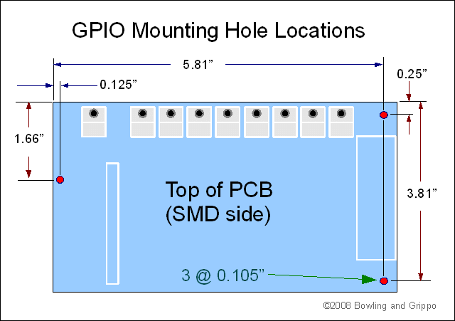
- PCB/case: Check the fit of the GPIO printed circuit board in the case. It goes into the next to last slots (nearest the case bottom). Do not put the GPIO PCB into the bottom grove, the bottom of this groove is wide enough that it may short out some circuits. Be sure to start it as close to 'square' as possible, otherwise it will bind. The PCB should slide into the case fairly easily, but be held snugly. If the PCB doesn't fit, or is too tight, you have to narrow the board slightly. you do this with a coarse file. Run it along
the heat sink edge of the board 10-20 times, then recheck the fit. Repeat as necessary until the board fits properly in the PCB. Then blow the PCB clean with compressed air. Note that if you wish to mount the GPIO PCB in a non-standard case, three mounting holes are provided:
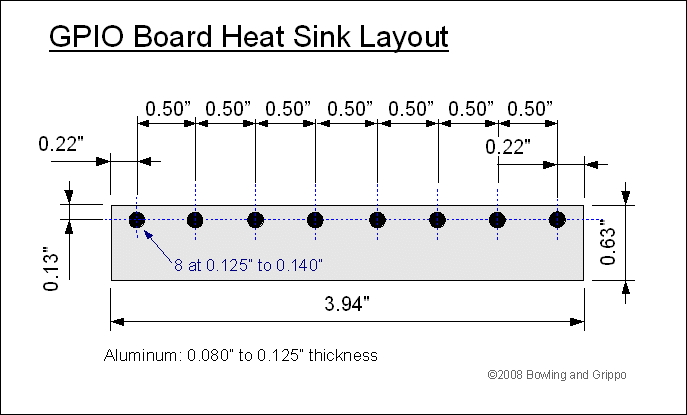
- Heat sink: Prepare the heat sink. You will make this out of 1/8" (3mm) aluminum flat strapping, 5/8" wide (15.8 mm) by 3.94 inches (100mm) long. You will drill 8 holes in it to match the PCB heat sink
area.
Because aluminum isn't typically sold in 5/8" widths, you may have to cut down wider aluminum (¾" or 1") to get a heat sink that will to fit. The easiest way to get the hole spacing right is to transfer the holes from
the PCB to the aluminum strip by placing them together and using a felt pen to mark the hole locations on the aluminum strip through the PCB.
Be sure to allow enough room for the aluminum strip to fit in the case and
allow enough room so that it won't contact the component leads. Make sure the heat sink rests up against the case when installed to get the thermal contact between the case and the heat sink. Sand both sides of the heat sink to ensure there are no burrs.
- Case End-Plates: Use this link 4L60E build Guide
for the connector end plate for the EAS-400 enclosure with both the V2.10 GPIO board and MegaSquirt® V3 main board in the same case.
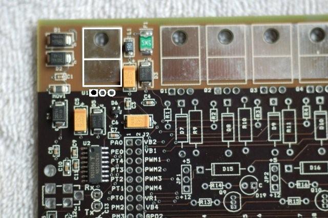
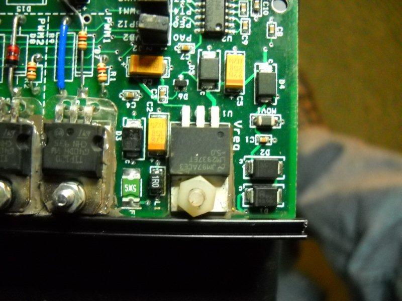
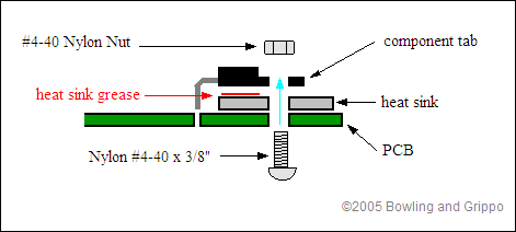
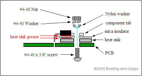
- Install and solder the voltage regulator U1 {LM2937ET-5.0-N}. This is a TO-220 size component (three pins sticking out of a black case, with a tab and mounting hole on the opposite edge) located in the corner of the board furthest from where the 35 position Ampseal connector will be installed, nearest the heat sink.
It has its own location among the SMD components in that corner of the board. You have to bend the leads to a 90° angle so the regulator can site flat against the board, then solder it and screw it the board with a #4-40 nylon bolt and nut (with heat transfer compound (aka. 'heat sink grease') between the regulator and board). You do not need a separate heat sink for the voltage regulator (shown in the diagram below), the voltage regulator can be mounted directly to the PCB (with heat sink compound), as long as you are not using the 5Vref supply for powering off-board accessory circuits.
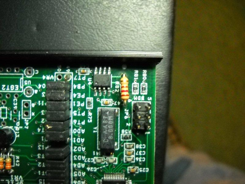
- CAN termination resistor: You will install this 120 Ohm, 1/4 Watt resistor (R82) if you have two CAN devices in your network (i.e. the GPIO board and MS-II). If you have more than two devices in the network, you only install the resistor in the devices at the ends of the CAN network. If required, install and solder the 120 Ohm, 1\4 Watt resistor {brown-red-brown, 120QBK-ND} in R82. This is located in the corner of the PCB furthest from the Ampseal connector and heat sink. Space the CAN termination resistor up off the board by
approximately 1/4" to 1/2" (6mm to 12mm), and make sure the lead closest the edge will not contact the case when the PCB is installed in the enclosure. If your board is not at the end of the CAN chain, DO NOT jumper this resistor location, leave it empty.
- Ampseal
- Connector: The connector should be soldered to th PCB. Be sure it snaps into place in the PCB, then solder each of the 35 pins from the underside of the board. Take your time and be methodical, as missing or poorly soldering one or more pins can cause problems that are very hard to troubleshoot late.
- Pigtail: The best instructions for assembling the harness pigtail are
Tyco's own instructions, get the PDF file here: Ampseal 35
pigtail assembly instructions
- Serial Communications:
You have a choice here. You can bring the serial communications out a serial jack (with a 2.5mm mini stereo jack, which is convenient) or you can bring the serial communications out the Ampseal connector (which offers the possibility of weather sealing).
- Ampseal Serial:
- Rx: Jumper from the via marked "Rx" near the bootloader jumper to the via marked "Rx" near the Ampseal connectors rear edge with 20-24 gauge insulated wire. This will bring Rx out on Ampseal pin 21.
- Tx: Jumper from the via marked "Tx" near the bootloader jumper to the via marked "Tx" near the Ampseal connectors rear edge with 20-24 gauge insulated wire. This will bring Tx out on Ampseal pin 22.
- Gnd: Use one of the Ampseal pins 17 to 20 as a ground.
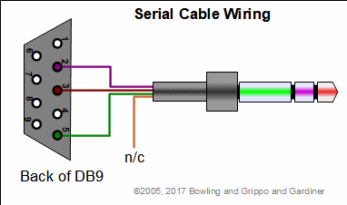
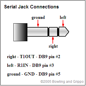
- You can devise your own serial cable, the illustrations below might help.
- Serial Jack/Cable
- Cable:(same as LC-1/MicroSquirt cable): If you don't already have a serial cable (from an MicroSquirt on Innovate LC-1 wide band EGO controller you will need to make one. To do this, solder the three wires of the 2.5mm stereo plug cable {CP-254CS-ND} to the DB9 connector {4109FER-ND} as shown below (cut the yellow wire so it can't short against the DB9 connector), then cover the connection with the DB9 hood {976-09RPE-ND}.
- Serial Jack: Solder the serial jack onto the PCB (near the enter of the edge of the PCB that is furthest from the Ampseal connector. The jack is available from Mouser as KC-300416 (161-2502), but it is not currently available from Digi-Key.
- Bootloader header {A26520-40-ND - cut to suit}: The Boot Header {JP5) on the board near the serial jack is used to reprogram the CPU in MegaShift™ processor (not the tuning parameters, but the actually code that uses the tuning parameters). Install the 2-position header, but leave it open (do not bridge the pins with a jumper), though you can leave a jumper (S9000-ND) hanging on just one pin as a handy storage location. Depending on what you want from your MegaShift™ controller, though, you may end up using the boot header to eventually to load code. To load new code you put jumper on the two pins on JP5 with no power applied to the board, and once the jumper is in place apply power to the board and use the downloader program.
Some people have put a momentary switch (normally open - NO) across the boot header, and place the switch so they can go into bootloader modes simply by pressing this switch while powering up, without opening the case. (if you do this, be sure it can't be pressed accidentally.)
- BDM (Background Debug Module) header: This 3x2 header is used to load the serial monitor program to the processor (to act as a bootloader for adding new code version), as well as for looking at the state of code running on the processor when developing new code (in conjunction with a BDM cable, etc.). This is located in the corner of the PCB furthest from the Ampseal connector and heat sink, near the CAN termination resistor (R82) you installed earlier. If you wish to install this header, solder it into position.
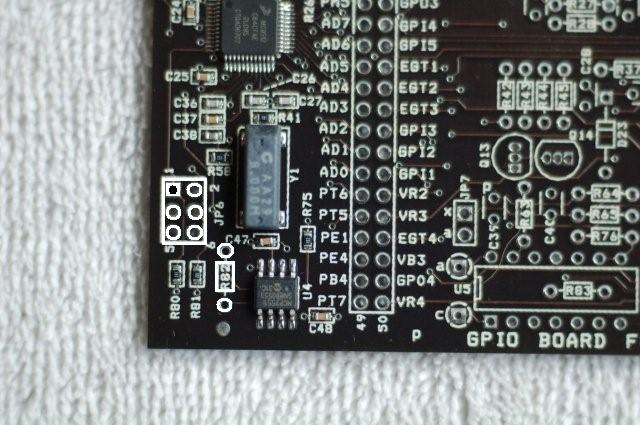
- 25x2 Header {WM8135-ND, S9000-ND}: Before installing the jumpers, you must use insulated wire (~20-22 gauge) to jumper:
- AD1 to GPI2 at the 25x2 header, and
- PT7 to VB1 at the 25x2 header.
Do these jumpers first, then cut the 25x2 header with small side cutters to fit remaining holes as necessary. Solder each of the header pins from the bottom side of the board (you can use tape to hold the header in place while it is upside down). Install jumpers on all the applicable circuit (see the table near the top of this document).
You can use snipped off leads as jumpers instead and save several dollars on the WM8135 header and jumpers - if you are doing this, wait until the end of the build to install the remaining jumpers - and save the snipped off leads from other components as you go.
(You could install the complete 25x2 header then jumper the relevant pins by soldering wires directly to the header pins, if you prefer. Be sue not to bridge adjacent pins, of course.)
Double check that you have jumpered the correct locations.
- Now that you have assembled the base circuits on your GPIO, you need to load the MShift™ code (loadable code files and instructions are listed here: Code Versions). Completing this step will verify that CPU and serial communications circuits are functioning.
B. Resistor Reference
|
Resistor Band Color Reference |
|
Color |
Band 1 |
Band 2 |
Multiplier |
Tolerance |
| Black |
0 |
0 |
x 1 |
not used |
| Brown |
1 |
1 |
x 10 |
not used |
| Red |
2 |
2 |
x 100 |
not used |
| Orange |
3 |
3 |
x 1000 =3D 1K |
not used |
| Yellow |
4 |
4 |
x 10000 = 10K |
not used |
| Green |
5 |
5 |
x 100000 = 100K |
not used |
| Blue |
6 |
6 |
x 1000000 = 1M |
not use |
| Violet |
7 |
7 |
not used |
not used |
| Gray |
8 |
8 |
not used |
not used |
| White |
9 |
9 |
not used |
not used |
| Gold |
not used |
not used |
divide by 10 |
=15% |
| Silver |
not used |
not used |
divide by 100 |
=10% |
| None |
not used |
not used |
not used |
=20% |
For example, this resistor:
| |
|
band1 |
|
band2 |
|
multiplier |
|
tolerance |
|
|
|
|
|
|
|
|
|
|
|
|
|
| |
|
|
|
|
|
|
|
|
|
|
|
|
|
|
|
|
|
|
|
|
|
Is 4.7K Ohms, since band1 is yellow=4, band 2 is violet=7, an the multiplier is red= x100, so we have 47x100 = 4700 Ohms = 4.7K Ohms. The tolerance is 10%. Note that you start reading at the end furthest from the gold or silver band.
C. VB3 (SolA), VB4 (SolB)
These two circuits are located on/beside the heat sink, nearest the Ampseal connector.
- Install and solder two large TO-220 size NPN transistors {TIP120-ND} in Q7, Q8 and insulators (under Q7, Q8 {4724K-ND}) on the heat sink in positions Q7, Q8. These are numbered alongside the 3 holes in the PCB for each transistor. You have to bend each transistor's leads to a 90° angle so the transistor can site flat against the insulator/heat sink. Cut the corners off the mica (nearest the three holes for the TIP120 pins) so that it clears the resistor you will install in the next step. Slide the mica over the TIP120's three pins and place it on the board. Then and screw the TIP 120 to the board with a #4-40 steel bolt insulator washer (be sure the stepped side is against the TIP120 tab), lock
washer and nut (with heat sink compound between the transistor and heat sink and heat sink and board). You may want to put a dab of fingernail polish or something similar on the screw/nut interface to help prevent them backing of
due to vibration. Alternately, you can use a nylon bolt without a insulating washer. The nut should be on the top side, to provide clearance in the case. Solder the TIP120 pins from the bottom side of the board.
Check the resistance from the TIP120 tab to the heat sink. It should be greater than about 40K Ohms (40000 Ohms), usually higher at this stage. If it is not greater than ~40K Ohms, the mica is not insulating, and you need to find out why (common causes are burrs on the heat sink, missing mica insulators, or missing insulating washers).
- Install and solder the transistor 1.0K Ohm, 1/8 Watt base resistors {brown-black-red, 1.0KEBK-ND} in R7, R8.
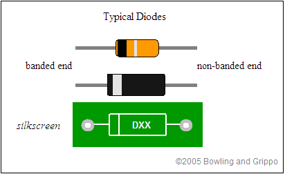
- Install and solder the 30V Zener diodes {1N4751ADICT-ND} in D13, D14. The banded end goes towards the heat sink, as shown on
the silkscreen.
|
Positive is:
|
|
Capacitors: |
LEDs: |
Diodes: |
|
The longer lead on polarized capacitors (not all are), sometimes marked with a small +
|
The longer lead on LEDs, and the lead opposite the flat on the case If you can see inside the LED, the cathode (which is on the same side the flat would be) is the larger electrode (but this is not an 'official' identification
method).
|
The end FURTHEST from the band (for forward conduction).
|
D. PWM1(Speedo Out), PWM2(TCC), PWM3(PC Sol):
These three circuits are located on/beside the heat sink, furthest from the Ampseal connector.
- Install and solder two large TO-220 size NPN transistors {TIP120-ND} in Q1, Q2, with insulators {4724K-ND} on the heat sink in positions Q1, Q2, Q3, . In Q3 (for the pressure control solenoid), solder in the similar looking RFP30N06LE-ND with an insulator.
These components are numbered alongside the 3 holes in the PCB for each transistor. Slide the mica over the TIP120/RFP30N06LE's three pins and place it one the board. You have to bend each of the transistor's leads to a 90° angle so the transistor can site flat against the insulator/heat sink. Then and screw the TIP 120 to the board with a #4-40 steel bolt, insulator washer (be sure the stepped side is against the TIP120/RFP30N06LE tab), lock washer and nut (with heat sink compound between the transistor and heat sink and heat sink and board). You may want to put a dab of fingernail polish or something similar on the screw/nut interface to help prevent them backing off due to vibration. Alternately, you can use a nylon bolt without a insulating washer. The nut should be on the top side, to provide clearance in the case. Solder the TIP120/RFP30N06LE pins from the bottom side of the board.
Check the resistance from the TIP120/RFP30N06LE tab to the heat sink. It should be greater than about 40K Ohms (40000 Ohms), usually higher at this stage. If it is not greater than ~40K Ohms, the mica is not insulating, and you need to find out why (common causes are burrs on the heat sink, missing mica insulators, or missing insulating washers).
- Install and solder 1.0K Ohm, 1/8 Watt transistor base resistors {brown-black-red, 1.0KEBK-ND} in R1, R2. For R3, install a jumper made from a snipped off lead in this position.
- Install and solder jumpers on R9, R10 and R11 using snipped off leads. (You can install 0.1 Ohm resistors (not included), such as Digi-Key MPR3-0.1J-ND at 79¢ each, in these positions if you wish to us an oscilloscope to view the output currents.)
- Install and solder 30V Zener Diodes {1N4751ADICT-ND}, D8, D9. The banded end goes towards the heat sink, as shown on the
silkscreen.
- To use the speedometer output, you will need to connect a 'pull-up' circuit in the spot for D7 to force the output to be high or low (i.e., no to "float"). To do this, you will need to use a voltage source and a current limiting resistor. You can do this by soldering one end of a ~1.0K Ohm 1/8 watt resistor {brown-black-red, 1.0KEBK-ND} in the banded end of the location, while leaving the other 'free' end of the resistor standing up from the board. Then you run an 18 to 22 gauge jumper wire from the 'free' end of that resistor to a voltage source, typically either 5 Volts or 12 Volts. You can source this voltage from a jumper on one of the GPOx circuit jumpers (JP1, JP2, JP3, JP4). If you are not sure which voltage to use, 12 volts is
usually safe and effective for most speedometers. You may have to experiment with different resistors to suit your speedometer's input needs.
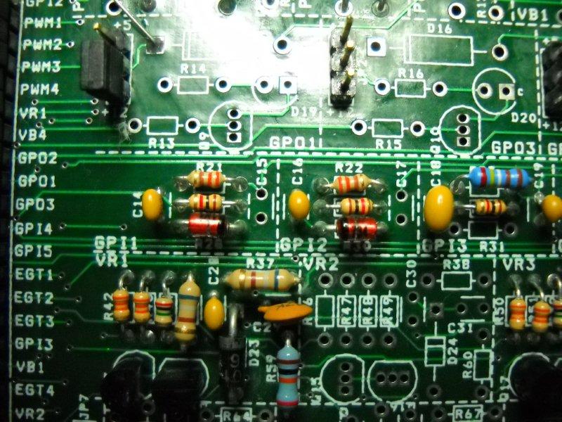
E. GPI1 (2/4wd sense), GPI2 (swB), GPI5 (DWNshift)
These circuits are arranged in a left-right line just above the center of the board. They are digital input circuits, and ground to activate (they have no internal pull-up, the GPIO must supply the pull-up circuit).
These circuits are arranged in a left-right line just above the center of the board. They are digital input circuits, and ground to activate (no pull-up).
Note, if you are not using a GM style shift lever input (3 digital inputs on swA, swB and swC) you can use swB and swC for datalogging analog voltage signals such as temperature or EGT. To do that, you need to build the circuits differently. See www.msgpio.com/manuals/gpi.htm for more details on different ways to build the GPI2 circuit. You can also use the 2/4WD input for logging digital inputs (if you don't have a 4WD), if you build the circuit appropriately and select the appropriate option in MegaTune.
- Install and solder a 1.0K Ohm, 1/8 Watt processor pin resistors {brown-black-red, 1.0KEBK-ND} in R27, R29, and R35.
- Install and solder 330 Ohm, 1/8 Watt resistors in R21 and R25. These are the pull-up resistors for the downshift button circuit on GPI5 and the 2WD/4WD switch on GPI1.
- Install and solder 5.6 Volt Zener Diodes in:
- R28 - banded end goes towards Ampseal connector,
- R30 - banded end goes away from Ampseal connector,
- R36 - banded end goes towards Ampseal connector.
- If (and only if) you are using the digital inputs for the manual gear lever determination such as with a 4L60E (as opposed to a variable voltage, Ford-style potentiometer) then you must add pull-up voltage to GPI2 (and EGT3 and EGT4 in later steps). Do this by installing a 330 Ohm resistor in R22.
- Install and solder 0.1µF capacitors {399-4329-ND} in C14 and C22.
- Install and solder a 0.001µF capacitor {399-4144-ND} in C16.
|
Capacitor Identification |
| Capacitors may be marked directly with their
capacitance. If not, they are frequently marked with numbers like:
104 K50 or 152 K100 The first two numbers
are multiplied by ten to the power of the third number to getting the
picofarad capacitance. For example, since 10 to the fourth power is
104 = 10 x 10 x 10 x 10 = 10,000, the first capacitor
would be 10*10,000 = 100,000pF = 0.1 µF, since 1,000,000pF =
1 µF. The second capacitor would be 15 x 102 = 15
x 100 = 1500pF = .0015 µF. The upper case letter indicates the
tolerance, M = 20%, K = 10%, J = 5%, H = 2.5% and F = ±1pF. The last
numbers are the rated voltage, 50 and 100 volts in these cases.
|
F. GPI3 (temperature)
This circuit is located near the center of the PCB. It is built as a voltage divider (resistance sensing) circuit.
- Install and solder a resistor, ¼ Watt, 2.49K Ohms {red-yellow-white-brown-brown (on blue), 2.49KXBK-ND} in R23. Space it off the board by about ¼" (6mm).
- Install and solder a 1.0K Ohm, 1/8 Watt resistor {brown-black-red, 1.0KEBK-ND} in R32.
- Install and solder a 1.0µF, 50V capacitor {399-4389-ND} in C18. You may have to straighten the leads somewhat to get them to fit the holes in the board. Do not let C18 touch R23 once assembled, bend it out of the way as necessary.
- Install and solder a 0.001µF, 100V capacitor {399-4202-ND in C19. Do not let in touch R23.
G. GPI4 (Brake sense)
This circuit is located behind the center of the Ampseal connector. This circuit is built as a digital input, but we must bring the nominal 12V stop lamp
voltage down to the 5V that the processor pin can handle (~6.5 Volts absolute maximum). R33 forms one leg of the voltage divider, and also limits the current through the Zener diode if the voltage is greater than 5.6 Volts.
- Install and solder a 15K Ohm, 1/8 Watt resistor {brown-green-orange, 15KEBK-ND} in R33.
- Install and solder a 10K Ohm, 1/8 Watt resistor {brown-black-orange, 10KEBK-ND} in R34.
- Install and solder a 5.6 Volt Zener diode {1N4734ADICT-ND} in place of C20, with the banded end towards heat sink. You will have to space it up off the board by about ½" (12mm) to get the leads to fit.
If the input voltage is 14.5 Volts, the voltage divider reduce this to 14.5 * 10K/(10K+15K) =3D 5.8 Volts, and the Zener diode further bleeds this off to 5.6 Volts (nominal) with a current of 14.5/15x103 = 0.97 milliamps (the Zener is rated for 1 Watt, which is much higher than we need which is ~1 milliamp * 0.2 Volts = 0.0002 Watts). If the input voltage is 11.5 Volts, the voltage divider reduce this to 115 * 10/(10+15) = 4.6 Volts, and the Zener diode does nothing. 4.6 Volts is till plenty to trigger the input pin (the acceptable voltage range for 'high' on a HCS12 input pin is 3.25 Volts or higher), which means the supply voltage from the brake signal could drop as low as 8.1 Volts and still trigger the input
successfully.
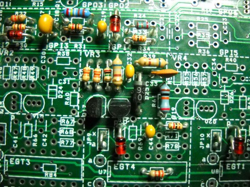
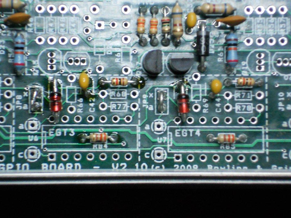
H. EGT3 (swC), EGT4 (swA) (If you need Non-CAN MAP see 4L60E build Guide).
Please note the the EGT circuits are arranged as EGT2, EGT3, EGT4, and finally EGT1 from left to right.
These circuits are located on the edge of the PCB furthest from the heat sink. They are built as voltage sensing circuits, to pass a 0-5V signal to the processor pin.
- Install and solder 1.0K Ohm, 1/8 Watt resistors {brown-black-red, 1.0KEBK-ND} in R67, and R70.
- Install and solder jumpers (made from snipped off leads) in JP8, and JP9.
- Install and solder 5.6 volt Zener diodes {1N4734ADICT-ND). These substitute in C41, and C43. The banded end goes closest to he the heat sink. You will have to space these about ½" (12mm) off the board to make the leads fit.
- Install and solder 0.001 µF capacitors {399-4202-ND} in C42 and
C44.
- If (and only if) you are using the digital inputs for the manual gear lever determination such as with a 4L60E (as opposed to a variable voltage, Ford-style potentiometer) then you must add pull-up voltage to EGT3 and EGT4 (and GPI2). To do this, install and solder 330 Ohm 1/8 watt resistors (330KEBK-ND} in R84 and R85, This is the pull-up voltage to EGT3 and EGT4 (and
GPI2).
I. VR1 (Vehicle Speed Sensor - VSS), VR3 (Input Shaft Sensor - ISS):
These circuits are built as a true VR 'zero-crossing' circuit, to convert the AC signal of a variable reluctor VSS/ISS sensors into a square wave signal for the processor.
Note that some of the VSS/VR1 components may need to be changed after assembly in order to get a clean VSS signal, depending on your installation. The details are on this page.
- Install and solder the small NPN transistors {2N304FS-ND} in Q13, Q14, Q17 and Q18 There is a fat side and a rounded side on these transistors. The flat side of Q13, Q17 and Q18. There is a fat side and
a rounded side on these transistors. The flat side of Q13, Q17 faces the Ampseal connector. The flat side of Q14, Q18 faces the
heat sink. The pin spacing is very tight on these components, be sure not to bridge them with excess solder. If you do bridge them, use a solder wick to
remove the excess solder. Make sure that Q14, Q18 does not touch the Zener diode in C40, C42 if installed.
- Install and solder 33K Ohm, 1/8 Watt resistors {orange-orange-orange, 33KEBK-ND} in R42, R43, R50 and R51.
- Install and solder a 2.0M Ohm, 1/8 Watt resistor {red-black-green, 2.0MEBK-ND} in R44, R52.
- Install and solder 300K Ohm, 1/8 Watt resistors {orange-black-yellow, 300KEBK-ND} in R45 and R53. Space it up off the PCB by about 1/4 inch (6 mm) in case you need to change it later. These resistor sets the trigger voltage on the VSS (R45) and ISS (R53) input circuits. The crossing point detection on the VR circuit may be biased too close to ground for some installations. However it is set up this way to pick up the VSS signal at the lowest speeds. However, the default trigger configuration might trigger on low-voltage noise in the signal. So you may need to change this resistor once you have MShift™/GPIO running in your vehicle. If you notice your speedometer and/or ISS jumps to very high values at low speeds, and adjusting the filtering options doesn't help, then you can try biasing the circuit(s) up a bit. The best way to do this for the VSS is to change R45 (VSS) and/or R53 (ISS) to a lower resistance. The specified value is 300K Ohms, and you can try from 47K to 220K to eliminate the false triggering on a noisy signal (the lower the resistance, the higher the trigger voltage). There are more tips on getting a clean VSS signal on this page.
- Install and solder a 10K Ohm, 1/4 Watt resistor {brown-black-range, 10KQBK-ND} in R59, R62.
- Install and solder 220K Ohm, 1/8 Watt resistors {red-red-yellow, 220KEBK-ND} in R37, R39.
- Install and solder a diode {1N4001DICT-ND} in D23and D25 with the banded end closest the heat sink, as shown on the silkscreen.
- Install and solder a 47 pF capacitor {399-4300-ND} in C28, C29, C32 and C33.
J. VR2 (UPshift button):
This circuit is located below the center of the board. It is built as a digital input (with a pull-up).
- Install and solder a 1.0K Ohm, 1/8 Watt resistor {brown-black-red, 1.0KEBK-ND} in R38.
- Install and solder a 5.6 volt Zener diode {1N4734ADICT-ND} in D24 with the banded end closest the heat sink as shown on the heat sink.
- Install and solder a 0.1µF capacitor {399-4329-ND} in C30.
- Install and solder a jumper (snipped lead) on R60.
- Install and solder a 330 Ohm resistor {330EBK-ND} from the hole for C31 (the "1" in C31 is partly obscured by the silkscreen for R50) closest the Ampseal connector to the hole for R48 (this spot is empty) closest the heat sink. This is the pull up resistor for the upshift circuit.
- Install and solder jumper insulated wire (~20-22 gauge) wire from the empty location of R49 (use the hole nearest the heat sink) to Q15 (to the pin nearest heatsink).
K. Finishing Touches
There are few more things to do before your board is finished and ready for use:
- Fit: Check the fit of the completed board in the case. Make sure that none of the TIP120 tabs contact the case. If they do, reposition them as required.
- Clean: This is a good time to clean the excess flux from the board. A common problem with boards that were
working and quit for no apparent reason is flux residue. Remove the processor. Wash your board with:
- 99% isopropyl alcohol (isopropyl alcohol is also known as "rubbing alcohol", and any drugstore will have it. Don't use the 70% isopropyl alcohol, it is much less effective), or
- acetone.
Lightly scrub both sides of the PCB with an old toothbrush. When cleaning flux, it is sometimes impossible to wash
it all off, some of it has to be scraped lightly to remove it. Use a round toothpick or wooden match broken in half for scraping the tough parts. This gives a small pointy end and large end to work with and reduces the chance of damaging the PCB. Be very careful not to damage the silk screen or traces. Rinse the PCB in hot water, then allow the PCB to dry completely. There should be very little haze left once it dries. Compressed air can speed the drying process, but be aware that some of the commercial compressed air cans have a solvent that can saturate any remaining flux and cause problems.
If there is still haze on the board after drying, or a white residue on any of the solder joints, you should rewash the board until these are completely eliminated. Note that because of the tight spacing of some of the SMD pins, the washing/drying is more critical on the GPIO board than it was on the V3 main board, for example.
- Test: Once the board is assembled and installed, you can test each circuit to be sure the signals are appropriate. For example, before installing the jumper for AD7/GPI4 (on the 25x2 header), look for an appropriate brake signal on the pin closest the Ampseal connector. The signal must be above ~3.25 V (but not more than 5.6V) to be 'high' and below about 1.75 Volts to be 'low'. Generally, you want to check each circuit that has the potential to have more than 5 Volts on it. If you are not sure, ask on the MShift™/GPIO forums.
- Jumpers: Once you are satisfied the circuits are within spec (that is, you are certain that NO 25x2 jumper pin will have more than 5.6 Volts on it at anytime, or you could damage the processor), you can install the jumpers for the circuits in the table below. The jumpers are on a 25x2 header. Each pair of pins is labeled with the processor pin on the left, and the circuit on the right. You need to install the jumpers to connect the circuits to the processor, otherwise you will not have the corresponding input/output functions enabled.
|
Transmission
Function |
Processor
Port |
GPIO
Circuit |
GPIO AMP
Connector Pin |
| Sol A |
PE4 |
VB3 |
23 |
| Sol B |
PM2 |
VB4 |
35 |
| TCC |
PT3 |
PWM2 |
32 |
| PC |
PT2 |
PWM3 |
33 |
| switchA |
AD0 |
EGT4 (build as GPI)1 |
26 |
| switchB |
AD1 |
GPI2 (jumper at 25x2 header) |
6 |
| switchC |
AD3 |
EGT3 |
25 |
| VSS output |
PT0 |
VR1 |
2 |
| VSS input |
PT5 |
VR3 |
14 |
| Temp Sensor |
AD2 |
GPI3 |
30 |
| Brake Sense |
AD7 |
GPI4 |
3 |
| Speedo Output |
PT4 |
PWM1 |
31 |
| 2WD/4WD Sense |
PE1 |
GPI1 |
5 |
(A few circuits are jumpered by wires, obviously these don't get a separate jumper across the adjoining pins.)
- Sealing: If you want to seal the finished board, use a conformal coating. Wait until you have cleaned and tested the board thoroughly though. If you do not think you will be doing much repair work on the board, you can not beat silicone conformal coating. It does require some digging to get it off for repair, however. Avoid the urethane coatings, as they are considered permanent and are a pain to try to work through.
You can also buy a spray can of acrylic lacquer conformal coating at most local electronics suppliers for around $10. If you are going to be working the board, “Krylon Krystal” clear spray works very well. Several coatings, preferably baked at 175-200°F degrees in between. This should slow down or prevent "solder bloom" and other deterioration of the PCB. Condensation is a fact of life for an outdoor component undergoing temperature changes. If needed, you can solder right through the Krylon Krystal and the residue cleans well with pure grain alcohol.
If you want to seal the finished board, use a conformal coating. Wait until you have cleaned and tested the board thoroughly though. If you do not think you will be doing much repair work on the board, you can not beat silicone conformal coating. It does require some digging to get it off for repair, however. Avoid the urethane coatings, as they are considered permanent and are a pain to try to work through.
You can also buy a spray can of acrylic lacquer conformal coating at most local electronics suppliers for around $10.00. If you are going to be working the board, Krylon Krystal clear spray works very well. Several coatings
preferably baked at 175-200°F in between. This should slow down or prevent "solder bloom" and other deterioration of the PCB. Condensation is fact of life for an outdoor component undergoing temperature changes. If needed, you can solder right through the Krylon Krystal and the residue cleans well with pure grain alcohol.
Testing your GPIO with MShift™
Now that you have assembled your GPIO, you need to load the MShift code (Code Versions), and test the installation.
If you have a trans stim, then you can test on the bench. If you don't have a stim and have wired the GPIO into the vehicle, you will need to do your testing there.
This page contains many suggestions for testing: Testing your GPIO with MShift™
MegaSquirt® and MicroSquirt® controller are experimental
devices intended for educational purposes. MegaSquirt® and MicroSquirt® controllers are not for
sale or use on pollution controlled
vehicles. Check the laws that apply in your locality to determine if using a
MegaSquirt® or MicroSquirt® controller is legal for your
application.
© 2010, 2015 Lance Gardiner and Dave Hjort. All rights reserved. MegaSquirt®, MicroSquirt®, and MegaShift™ are registered trademarks.