MegaShift™ V2.00 Transmission Stimulator
These are the instructions to build a V2 transmission stimulator (aka. TranStim™), using a PCB and the BOM parts. If you have any questions at any point, ask them at MShift™ forum.
1. Inspect the both sides of the printed circuit board (PCB) for any obvious damage. A bit of discoloration on some plated pads is normal, and will clean up when soldered. If you see any other damage, contact the vendor that sold you the PCB.
2. Use a multimeter to check the resistance between the 12V and 5V through hole pads for the 12 pin header, between the 12V and any of the large mounting hole pads, and between the 5V and any of the large mounting holes pads. All of these should have infinite resistance.
If you have less than 'infinite' Ohms between 5V and 12V (i.e. the same reading as with the probes held apart in the air and neither touching anything else), you must make a small fix to a trace on the board. You will need to cut a trace on the board, on the 555 integrated circuit (IC) pad, but on the bottom side of the board. The trace runs from pin 4 to a 'via' just off the pad (a 'via' is a pad that connects a trace on one side of the PCB to a trace on the other side of the PCB).
The red line in the illustration below shows where to make the cut.
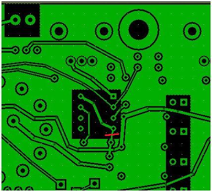
An early batch of TranStims™ had this trace, later ones do not. If the trace is there, it must be cut.
Do not cut the wider trace beside the one shown. It may be safest to cut from right to left (based on the above illustration). The cut doesn't have to be deep as the trace is only a few thousandths of an inch thick, and the cut doesn't have to be wide - just the width of a sharp blade is sufficient.
Make sure that you have infinite resistance between the 12V, 5V and ground points before proceeding. If you don't get infinite resistance, redo the cut.
3. Install and solder the 555 socket (3M5473-ND) onto the top of the board. Align the notch in the socket with the notch in the outline on the silkscreen. Solder it from the bottom side - you can use a piece of tape to hole it in place while you flip the board over. (In all cases, you insert the component from the top side of the PCB (the side with the silkscreen) and solder it from the bottom side, so we won't keep repeating that.)
4. Install and solder the 2N3904 transistor (2N3904FS-ND) in the pad location adjacent the 3-4 gear switch position. Looking at the PCB pad so the majority of the silkscreen printing is right side up, the through-holes are ground - signal - 12V. We want to connect ground-emitter, signal-base, and 12V-collector. Looking at the transistor from the top, with the curved side up and the flat side down, the pins are E-B-C. So install the transistor with the curved side closest to the edge of the PCB. You will have to spread the leads apart slightly to fit them in the holes. Solder the leads from the underside of the PCB. Snip off excess lead length from the underside of the PCB (do this for any component that has excess lead length for the remaining steps, we won't keep repeating this).
5. Install and solder the 12 position terminal block (ED15524-ND). Make sure to orient the wire ports facing outwards from the PCB.
6. Install and solder the 2 position SP1/SP2 terminal block (ED2635-ND). Orient the wire ports so they face outwards from the PCB.
7. Install and solder the 2 position SGNL/GND terminal block (ED2635-ND). Orient the wire ports so they face outwards from the PCB.
8. Install and solder the 4 position LED terminal block (ED2637-ND). Orient the wire ports so they face outwards from the PCB.
9. Install and solder the 4 position BRK/VSS/DWN/UP terminal block (ED2637-ND). Orient the wire ports so they face outwards from the PCB.
10. Install and solder the red push-button brake switch (EG4789-ND) in the BRAKE switch location. Be careful to orient the switch so that the grooves/tabs run 'side-to-side' on the PCB. That is, the switch is installed so that the grooves and tabs on the side of the switch are aligned with the terminal blocks on either side of the switch. Check the photo at the top of this page for clarification. If you get this wrong, the switch won't work so check it carefully before soldering.
11. Install and solder the green push-button upshift switch (EG4790-ND) in the UP switch location. Be careful to orient the switch so that the grooves/tabs run 'side-to-side' on the PCB. If you get this wrong, the switch won't work so check it carefully before soldering.
12. Install and solder the black push-button downshift switch (EG4788-ND) in the DWN switch location. Be careful to orient the switch so that the grooves/tabs run 'side-to-side' on the PCB. If you get this wrong, the switch won't work so check it carefully before soldering.
13. Install and solder LED current limiting resistors R1, R2, R3, R4, R5, R6, R7, R8, R9, R10, R11 and R14. These are all 470 Ohm ¼ Watt resistors (470QBK-ND). Resistors do not have a polarity, and can be oriented either way.
14. Install and solder Light Emitting Diodes D1, D2, D3, D4, PC, TCC, OUT1, OUT2, OUT3, SP1, SP2, and VSS (67-1102-ND). The short lead of each LED has a flat on the base of the LED on the same side. This is the 'cathode' and is the negative side of the LED. In all cases the cathode is marked by a flat spot on the silkscreen, and this is always on the left side of the LED pad (and is also marked by a square pad).
15. Install and solder the shift logic diodes D5, D6, D7 and D8 (1N4001DICT-ND). The end of the diode closest the band goes to the end of the component pad nearest the band on the silkscreen. In all cases this is nearest the 'V.200 TransStim' text on the PCB.
16. Install and solder the 1.0K Ohms, 1/6 Watt R12 and R13 resistors (1.0KEBK_ND). These are located adjacent the 555 socket you installed earlier.
17. Install and solder the 10000pF capacitor C1 (490-3860-ND). This is adjacent the R5 resistor, and near the PC LED you installed earlier. This capacitor does not have a polarity, and can be oriented either way.
18. Install and solder the 100000pF capacitors C2 and C3 (490-3859-ND). C2 is beside C1 that you installed in the previous step. C3 is located between the 'OUT1' label for the LED and the 'V2.00 TransStim' label near the middle of the PCB. These capacitors do not have a polarity, and can be oriented either way.
19. You have a choice to make on the function of the 0-5V stim. This pot can be configured for variable resistance (a Ford shifter, for example) or a 0 to 5 Volt signal (non-CAN load or other uses).
You can install a header (929834E-01-02-ND) and jumper (2-881545-2-ND) in the jumper location so you can switch back and forth between the 5V and resistance signal, if you like. The most recent BOM includes these components, so install the header, and put the jumper across both pins if you want a 0 to 5V signal, and on just one pin if you want a variable resistance.
20. Install and solder the two 10K pots for TEMP and 0-5V (P3A1103-ND) controls. Solder the thee pins that are in a row - you don't have to solder the large pins on the side of the pots (which are just for mechanical support) but it doesn't hurt to solder them either.
21. Install and solder the 1.0M pot for VSS (CT2271-ND).
22. Install and solder the 6-position rotary switch (EG1953-ND). If you look at the underside of the switch, you will see the pins are numbered. Put pin #2 towards the large '2' in text meant to indicate 2nd gear. You may have to bend the pins slightly to fit the holes. The pins are a tight fit in the holes, you will have to use a fair bit of force to seat the switch before soldering.
23. Install the 555 chip (LM555CNFS-ND) into the socket you installed in step 3. Be sure to align the notch in the chip with the notch in the socket. Make sure the leads are started into the socket (you may have to adjust them for width a bit), then press the chip into the socket firmly.
24. Put four 3/16" (#10) by 1" to 2" long bolts in from the top of the PCB, and lock them in place with nuts from the other side. You can buy these bolts in any hardware store. These will raise the stim off the surface it rests on, reducing the likelihood of accidental shorts. These screws are grounded, so they also make a good spot to attach a oscilloscope probe's ground clip(s).
25. Wash the completed board in 99% isopropyl alcohol (available at any drugstore), and scrub it lightly with an old toothbrush until all the residual soldering flux is removed, then rinse it well in hot water, and let it dry for several hours.
| Function | Ampseal Pin | TransStim | Location |
| Temperature Sensor High | 30 | T1 | 12-pos term. block |
| Temperature Sensor Low | 17 | T2 | |
| 12V Supply | 1 (both to 12V source) | 12V | |
| Line Pressure Control (aka. 'Force Motor') | 33 | PC | |
| Torque Converter Clutch | 32 | TCC | |
| Output 1 | 23 | OUT1 | |
| Output 2 | 35 | OUT2 | |
| Output 3 | 34 | OUT3 | |
| 5 Volt Reference | 28 | 5V | |
| Input 1 | 26 | IN1 | |
| Input 2 | 6 | IN2 | |
| Input 3 | 25 | IN3 | |
| Signal | multi-use variable voltage/variable resistance controlled by 0-5V pot | SGNL | 2-pos term. block |
| Ground | 18, 19, or 20 (shared with ground for 12V source) | GND | |
| Spare Port 1 | 11 | SP1 | 2-pos term. block |
| Spare Port 2 | 12 | SP2 | |
| Brake | 3 | BRK | 4-pos term. block |
| Vehicle Speed Sensor | 2 | VSS | |
| Downshift Button | 4 | DWN | |
| Upshift Button | 15 | UP | |
| Gear Indicator LED 1 | 10 | 1 | 4-pos term. block |
| Gear Indicator LED 2 | 7 | 2 | |
| Gear Indicator LED 3 | 8 | 3 | |
| Gear Indicator LED 4 | 9 | 4 |
| Gear | IN1 | IN2 | IN3 |
| R | low | low | HIGH |
| N | HIGH | low | HIGH |
| 4 | HIGH | low | low |
| 3 | HIGH | HIGH | low |
| 2 | HIGH | HIGH | HIGH |
| 1 | low | HIGH | HIGH |
If you want the shifting to match the pattern on the PCB (1-2-3-4-N-R clockwise) leave these at the defaults. You may need to change these in the vehicle (unless you are using a 4L60E transmission).
The rotary shift switch has a second independent pole, and the connections for this are brought out below the switch in a 0.100" header labeled 'RN4321'. The circled J7 hole at the end is ground for the switch's second pole. You can build any shift circuit logic you like and connect to this header.

Set the 'Max. Vehicle Speed' very high (250 or 300 mph). If the VSS input exceeds the Max. Vehicle Speed, the speedometer will bounce crazily. It's fairly easy to exceed the Max. Vehicle Speed with the stim's VSS circuit (unlike in the vehicle!). So try to get the Max. Vehicle Speed well above any speed you will use, and if the speedometer starts bouncing, try turning the VSS pot clockwise until it stops.
BTW, be sure the stim's ground is connected to the GPIO board's ground, or the signal could be quite noisy. You can run a ground test lead from any of the #10 screws to a ground on the GPIO board (such as the non-banded end of D12.