A quick note for those getting test production V2.00 GPIO boards:
There is a small error in the silkscreen labeling at the 25x2 header (that connects the processor pins to the circuits). The processor side labels are correct, only the circuit side has errors. The affected circuits are:
pin/port -- labeled ---- actually
PAD00 ---- GPI1 ------- EGT4
PAD01 ---- GPI2 ------- VB1
PE0 ------- VB1 -------- GPI2
PE1 ------- EGT4 ------ GPI1
Note that these were the assignments on the beta boards, they were changed when Bill laid out the production boards.
This will be noted in all build instructions, but be aware of it if you are doing your own circuits.
Lance.
V2.00 board errata
-
Bernard Fife
- Posts: 1696
- Joined: Fri Apr 04, 2008 1:28 pm
V2.00 board errata
"Never wrestle with pigs. You both get dirty and the pig likes it." - George Bernard Shaw
-
Bernard Fife
- Posts: 1696
- Joined: Fri Apr 04, 2008 1:28 pm
Re: V2.00 board errata
Not exactly an error, but something to be aware of, the EGT circuits are arranged as:
EGT2 -- EGT3 -- EGT4 -- EGT1
also, the GPO circuits run:
GPO1 -- GPO3 -- GPO2 -- GPO4
from left to right on the board. The component numbering matches the schematics, etc.., but people should not assume they are 1-2-3-4 in physical order on the board like they wee on the beta boards.
Lance.
EGT2 -- EGT3 -- EGT4 -- EGT1
also, the GPO circuits run:
GPO1 -- GPO3 -- GPO2 -- GPO4
from left to right on the board. The component numbering matches the schematics, etc.., but people should not assume they are 1-2-3-4 in physical order on the board like they wee on the beta boards.
Lance.
"Never wrestle with pigs. You both get dirty and the pig likes it." - George Bernard Shaw
-
Bernard Fife
- Posts: 1696
- Joined: Fri Apr 04, 2008 1:28 pm
Re: V2.00 board errata
All,
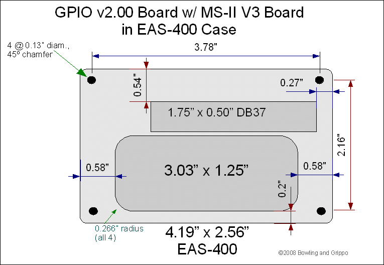
Another thing to be aware of: in the re-layout of the board for production (as V2.00), some via and component locations were moved closer to the 'long' edges of the board. Because the bottom of the bottom slot of the EAS-400 is wider than the other slots, this means the GPIO PCB can no longer go in the bottom slot. As a result, the GPIO and MS V3 PCB will no longer fit into an EAS-400. The EAS-500 is much wider (6 inches) so we'll have to scratch our heads for a bit on this one.
In the meantime, users can use an EAS-400 to house the GPIO board individually (it won't fit in a EAS-300 and still have room for the Ampseal connector unless put in the bottom slot, which is not recommended, as noted above).
Lance.
"Never wrestle with pigs. You both get dirty and the pig likes it." - George Bernard Shaw
-
Bernard Fife
- Posts: 1696
- Joined: Fri Apr 04, 2008 1:28 pm
Re: V2.00 board errata
All,
It looks like the components that are too close to the slots are primarily those not used in building the MegaShift hardware (it's the EGT AD595 IC pins that are the closest), so that helps, it *could* go in the bottom slot.
However, there's another problem - the board was made 6.00" x 4.00", but it need to be 5.89" x 4.00" to allow for the Ampseal flange behind the end-plate. There doesn't appear to be enough room to remove this from the other end of the PCB to compensate. We'll put our heads together on this one and let people know what we will do. BTW, there are 4 locations on the board for 'stand-off' mounting, I will illustrate these locations in the build guide shortly: http://www.msgpio.com/manuals/mshift/assembly.html
Lance.
"Never wrestle with pigs. You both get dirty and the pig likes it." - George Bernard Shaw
-
Bernard Fife
- Posts: 1696
- Joined: Fri Apr 04, 2008 1:28 pm
Re: V2.00 board errata
One way around the board length issue is to cut the end plate around the Ampseal flange. That means the connector is not weather-proof anyore, of course...
"Never wrestle with pigs. You both get dirty and the pig likes it." - George Bernard Shaw
-
Bernard Fife
- Posts: 1696
- Joined: Fri Apr 04, 2008 1:28 pm
Re: V2.00 board errata
In fact, if the end plate around the Ampseal flange (mentioned above) is 0.100" to 0.110" thick, then a 'proper' end plate can be put over that to form a sealed unit. I will post drawings of these shortly.
Lance.
Lance.
"Never wrestle with pigs. You both get dirty and the pig likes it." - George Bernard Shaw
-
Bernard Fife
- Posts: 1696
- Joined: Fri Apr 04, 2008 1:28 pm
Re: V2.00 board errata
All,
Here is the recommended end-plate dimensions for putting a V3 main board and v2.00 GPIO in the same enclosure:
There's more details in the MegaShift assembly manual. I will put more drawings in the assembly manual shortly (GPIO only in an EAS-400), and plate dimensions for the other end-plate.
Lance.
"Never wrestle with pigs. You both get dirty and the pig likes it." - George Bernard Shaw
-
Bernard Fife
- Posts: 1696
- Joined: Fri Apr 04, 2008 1:28 pm
Re: V2.00 board errata
All,
I discussed this with Bruce, and we will correct the 'board length' issue (as well as fix the slkscreen labeling of a few circuits) for the next run of GPIO boards. So those that have the test boards can use the above end-plate design, while those with subsequent boards will have a separate end-plate design (which I will put in the manual shortly).
BTW, I have added info to the build guide regarding how to bring the serial comms out through the Ampseal connector instead of the mini-stereo jack: http://www.msgpio.com/manuals/mshift/assembly.html
Lance.
"Never wrestle with pigs. You both get dirty and the pig likes it." - George Bernard Shaw
-
Bernard Fife
- Posts: 1696
- Joined: Fri Apr 04, 2008 1:28 pm
Re: V2.00 board errata
All,
I have put the latest BOM here:
http://www.megamanual.com/mshftbom.htm
The latest build guide is here:
http://www.msgpio.com/manuals/mshift/assembly.html
Both of these are reasonably complete and correct (I have just used them to assemble a board), but they likely aren't perfect (we will fix them up as people report errors, of course).
I am going to start testing the I/O circuits on the production board next.
Lance.
"Never wrestle with pigs. You both get dirty and the pig likes it." - George Bernard Shaw
-
Bernard Fife
- Posts: 1696
- Joined: Fri Apr 04, 2008 1:28 pm
Re: V2.00 board errata
All,
Please note that some of the 5.6 Zener diodes are marked Cxx in the BOM because they physically install in the place of those caps on the board (so it din't make sense to me to give them a Dxx designation, only to later instruct users to install them in Cxx locations!).
Also, I forgot to put EGT3 (built as a digital input) into the BOM and build guide. I have done that now, but you might be short one 5.6 Zener (in C42) and one 0.001 uF cap (in C41) for that circuit if you have already a previous BOM. (There should be extra 1.0K resistors to complete the circuit.) The cap is optional, the Zener and resistor are not.
I also added links to the general EGT and GPI circuit build guides for those using the 'Ford' (voltage based) gear lever position determination, since these two circuits (for swB and swC) can be used for other purposes - like temperature or EGT or MAP or ... (the gauges and logging are already built into MegaTune, etc.)
I don't have enough info yet to program the LU Feel solenoid. However, I am adding upshift and downshift ignition timing retard, as well as gear based timing retard (for 2nd, 3rd, and 4th gear) for use with MS-II.
Lance.
"Never wrestle with pigs. You both get dirty and the pig likes it." - George Bernard Shaw